
Sharing one ADC across multiple sensors: analog switches from SGMICRO and 3PEAK
Designers adding temperature, voltage and pressure measurements to a board face a familiar trade-off: a separate ADC for every signal takes space, power and budget. Routing the signals through a multiplexer lets them share one converter, provided the circuit gives each channel enough time to settle.
For engineers assessing suppliers in China, SGMICRO and 3PEAK offer several channel arrangements and supply ranges in their 2026 documentation. These parts are candidates for different acquisition paths. Their usefulness depends on the signal source, ADC input and scan schedule as much as the switch itself.
1. Allocate acquisition time before choosing the channel count
Temperature scanning and power monitoring often measure relatively slow signals in sequence. The controller selects a channel, allows the analog path to settle, then lets the ADC acquire and convert the input before selecting the next channel. This can be an economical arrangement when many measurements share modest update-rate requirements.
Applications that compare phase or fast transients at the same instant need to consider simultaneous sampling. An external multiplexer increases the number of connected inputs; those inputs still share the ADC's acquisition time.
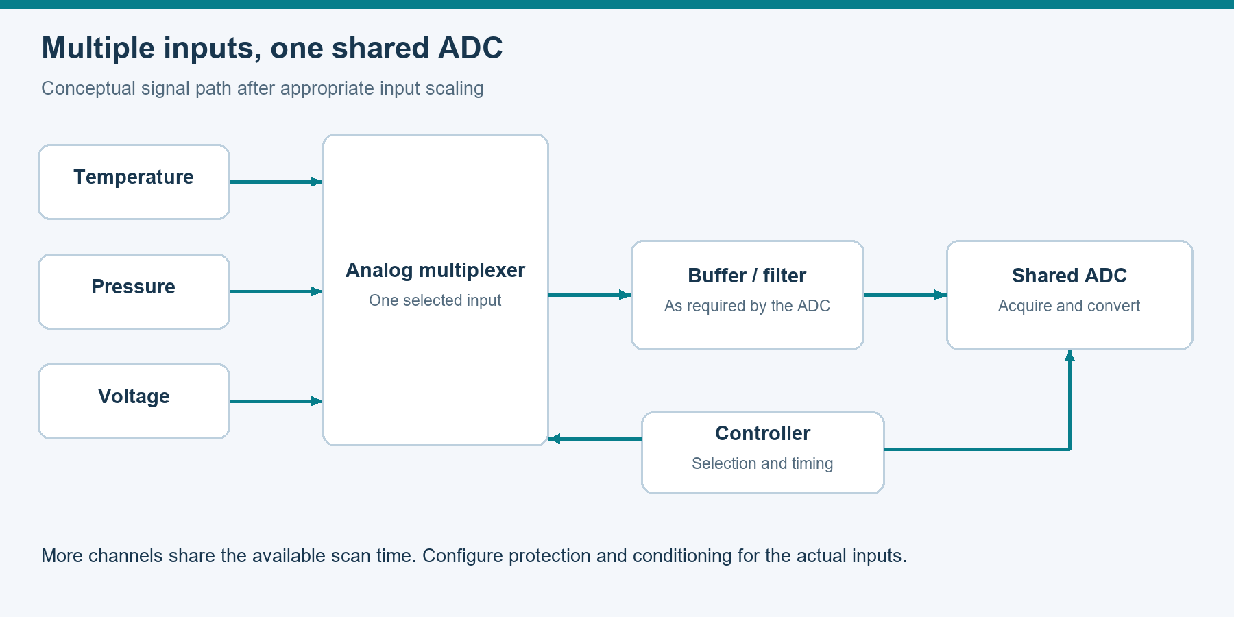
Figure 1. Multiple analog inputs share one ADC. Configure protection, signal conditioning and drive circuitry for the sensor outputs and the ADC requirements.
Adding channels lengthens a complete scan. Switching, settling and any required digital processing consume part of the available time. Defining the required update interval for each signal gives channel count and speed specifications a practical meaning.
2. Four devices cover different signal-routing requirements
SGMICRO's SGM4523 has a dual 4:1 configuration and a 1.62 V to 5.5 V supply range. Its two switch banks share address controls, with each bank connecting one of four inputs to its common terminal. This arrangement suits paired signal paths; it has a different connection structure from a single 8:1 multiplexer.
The May 2026 documentation also specifies injection-current control, back-power protection and fail-safe control inputs. Those functions merit evaluation where supplies start at different times or an unselected branch can see an abnormal voltage. Pin voltage and current ratings define the applicable conditions.
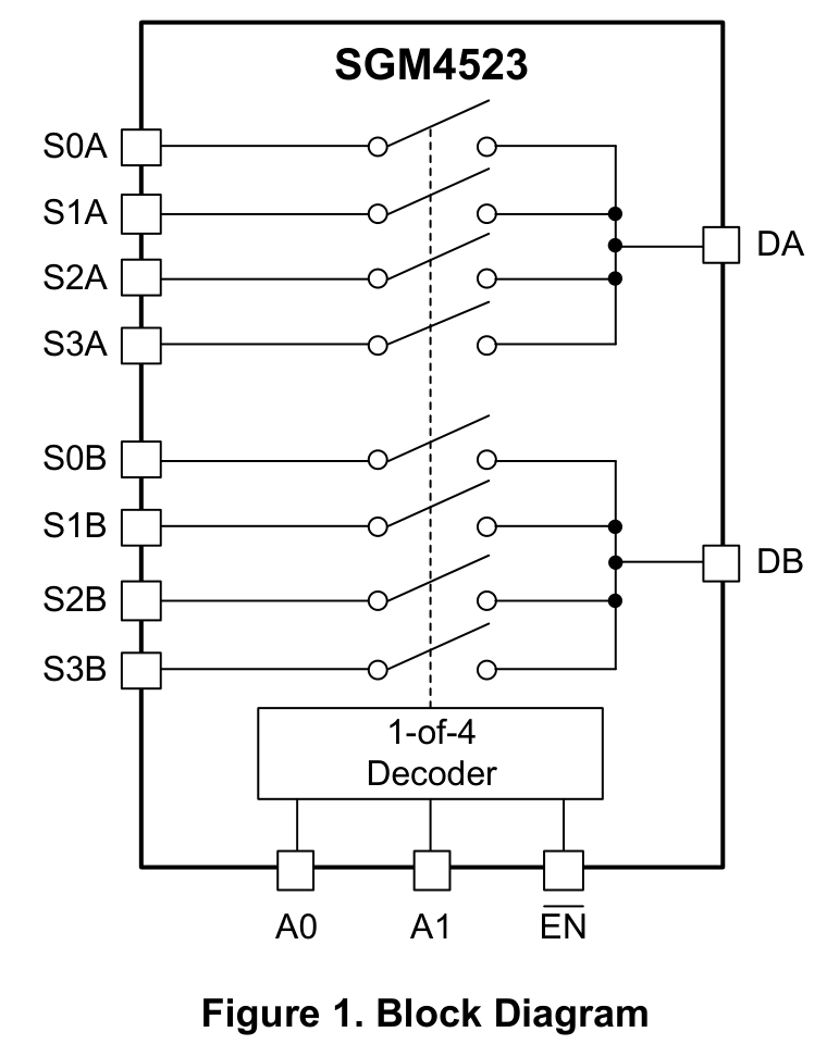
Figure 2. SGMICRO SGM4523 block diagram, reproduced from page 5 of the May 2026 Rev. A datasheet. The two 4:1 banks share address controls.
3PEAK's TPW3188 is a single 8:1 multiplexer operating from 1.65 V to 5.5 V. The company's 2026 analog selection guide lists it as a production device, making it a candidate for scanning multiple low-voltage analog signals.
Signals that go negative or exceed a low-voltage switch's operating range require another supply arrangement. The TPWH4051, also listed in that guide, provides an 8:1 configuration with a total positive-to-negative supply span of 4.5 V to 24 V. Analog signals remain within its supply rails, and the circuit must scale them appropriately before they reach the ADC.
| Supplier and device | Configuration | Documented supply range | Evaluation focus |
|---|---|---|---|
| SGMICRO SGM4523 | Dual 4:1 | Single supply, 1.62 V to 5.5 V | Paired paths and abnormal conditions on other branches |
| 3PEAK TPW3188 | Single 8:1 | Single supply, 1.65 V to 5.5 V | Scanning low-voltage inputs |
| 3PEAK TPWH4051 | Single 8:1 | Total supply span, 4.5 V to 24 V | Wider-amplitude and bipolar signals |
| SGMICRO 74HC4067 | Single 16:1 | Single supply, 2 V to 12 V | More inputs and allocation of scan time |
These are supply specifications. Check the ADC input limits separately. Sources are SGMICRO's February and May 2026 datasheets and 3PEAK's 2026 selection guide.
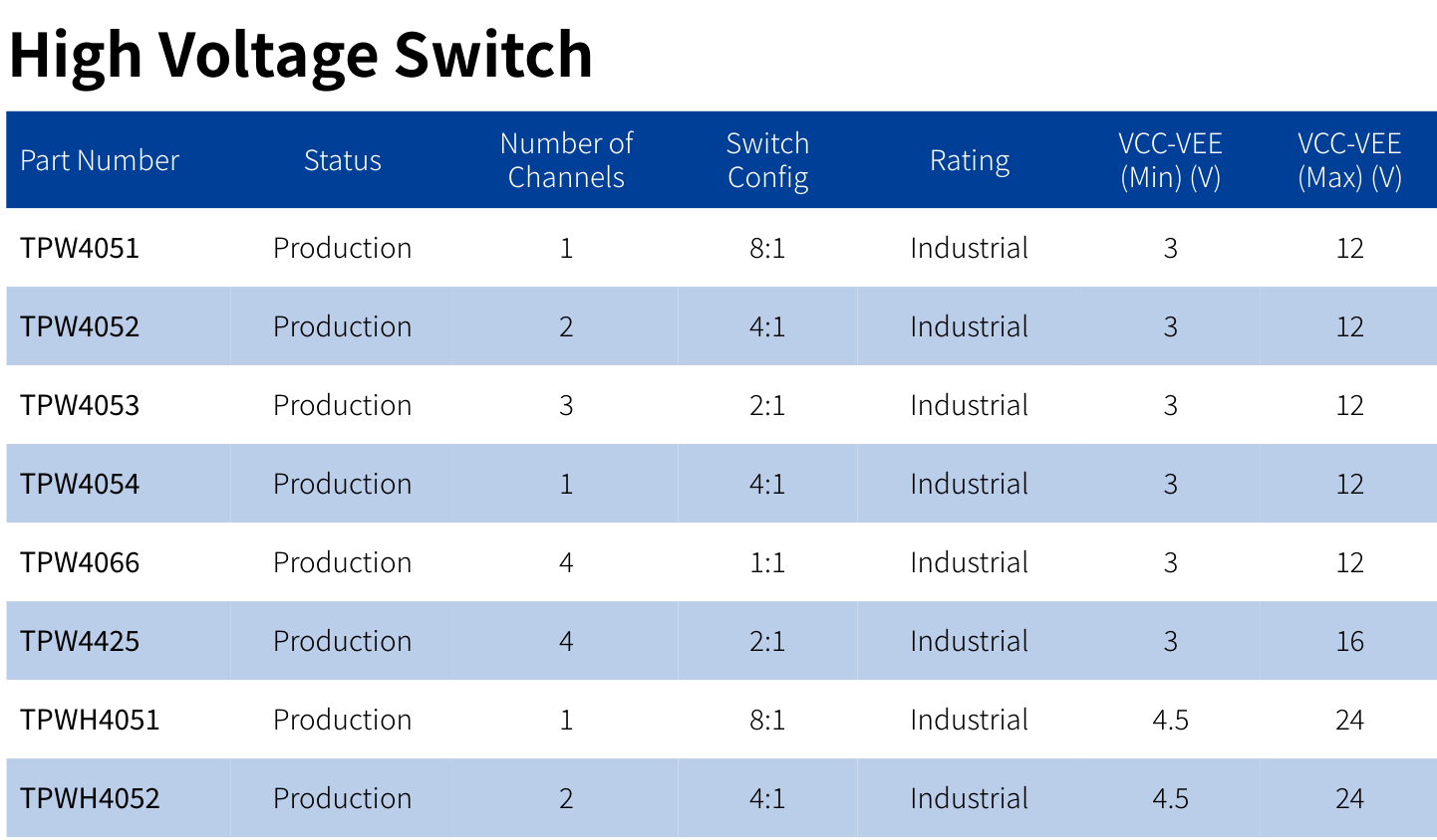
Figure 3. An excerpt from printed page 30 of the 3PEAK 2026 selection guide shows switch configurations, supply spans and product status. Inclusion in the guide does not establish a product's original launch date.
For larger input counts, SGMICRO's 74HC4067 provides 16:1 routing. Its February 2026 datasheet specifies a 2 V to 12 V supply range. Choose the channel arrangement and signal range first, then compare electrical characteristics under the intended conditions.
3. Build leakage and switching disturbances into the error budget
On-resistance is often the first switch parameter engineers compare. Its effect depends on the load. A high-impedance input may suffer little static divider error, while an ADC's sampling capacitor makes switch resistance and source impedance part of the charging path.
On-resistance also changes with supply and signal voltage. SGMICRO's 74HC4067 datasheet lists typical values of 220 Ω at a 2 V supply, 86 Ω at 5 V and 60 Ω at 10 V. Comparing numbers measured at different supply voltages can lead to a misleading choice.
Leakage deserves particular attention with high-impedance sources. As an illustrative calculation, 1 nA flowing through an equivalent source resistance of 100 kΩ corresponds to about 100 μV of offset. This is not a measurement of any device discussed here. It explains why maximum leakage at elevated temperature belongs in a precision design review.
Switching also injects charge into the output node and can cause a short voltage step. Charge injection during switching and the SGM4523's injection-current control address different effects: the former concerns a switching transient; the latter concerns current injected through an abnormal branch.
On-resistance, leakage and switching disturbances all belong in the acquisition error budget. Additional filter capacitance may reduce some transients while increasing settling time. A buffer changes the balance of drive capability, noise and power consumption.
4. Verify settling at the ADC input
Alternating between a near-full-scale channel and a near-zero channel is a useful test. After each transition, charge on the switch and downstream capacitances redistributes, and the amplifier and ADC input must settle again.
Datasheet turn-on time is normally measured with a specified load and output threshold. A high-resolution ADC can require a much smaller residual error. Completion of switching does not establish that the ADC input has reached its required accuracy.
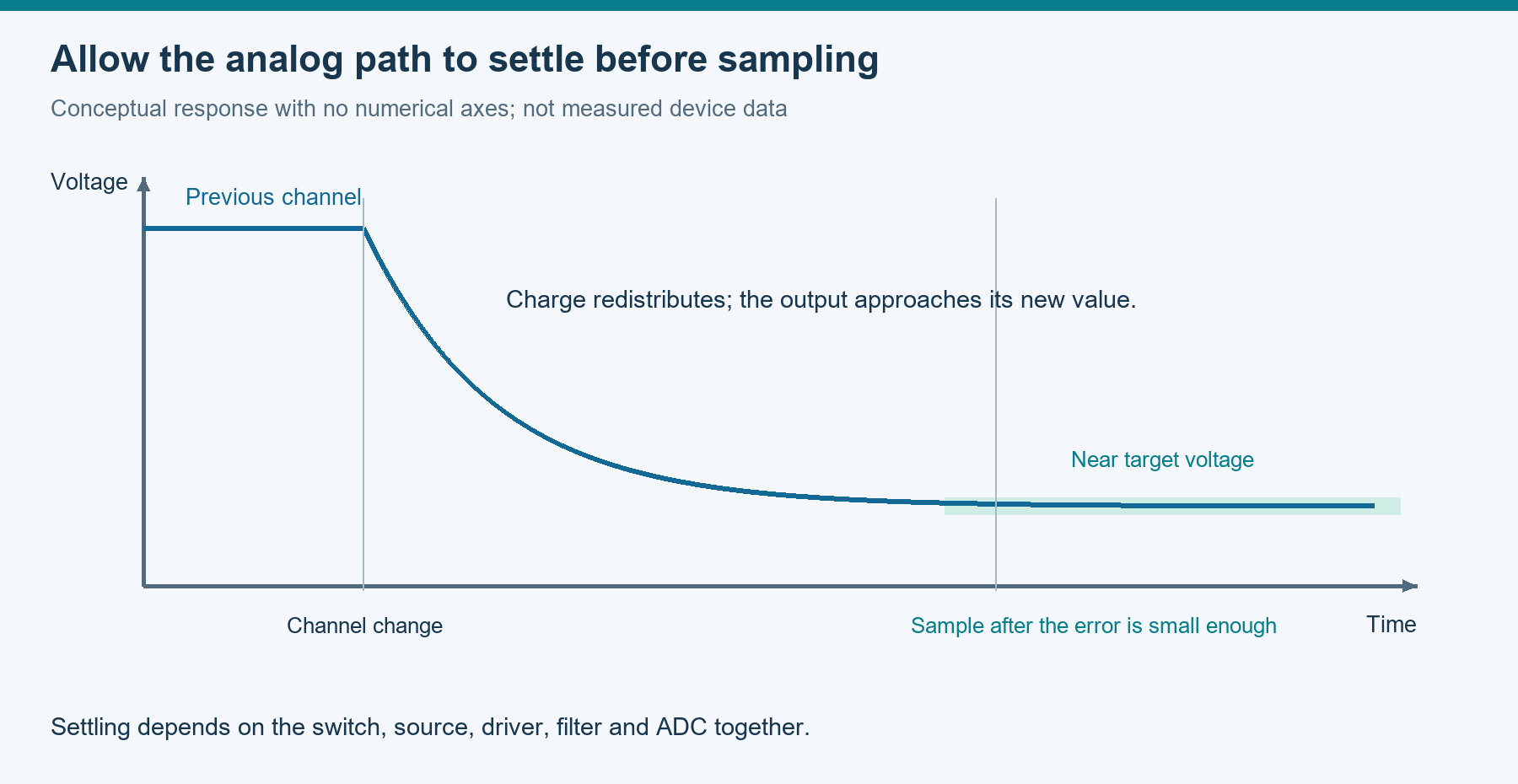
Figure 4. A conceptual settling response after a channel change, without numerical axes. It is not a measured device waveform. The complete circuit's error requirement determines the sampling instant.
Start validation by alternating high and low input levels and comparing the first reading after a switch with subsequent readings. Reduce the waiting time gradually, then vary source impedance, temperature and scan order to find the worst deviation. If the ADC uses digital filtering, include its response to a channel change in the timing budget.
Supplier qualification should identify the complete ordering code, package, temperature grade and supply status. Pin assignments and control logic must also match the target circuit. Those details make sample testing repeatable and make results useful to procurement.
SGMICRO and 3PEAK's current documentation provides choices from dual 4:1 through 8:1 to 16:1. A practical evaluation starts with a defined group of sensor channels: match the voltage ranges, calculate the expected errors, and use measured readings to establish the time each channel needs.