
Silicon capacitor newcomers: from product launch to repeatable supply
In May 2026, Samsung Electro-Mechanics disclosed a silicon capacitor supply agreement worth KRW 1.557 trillion. Delivery is scheduled from January 2027 through December 2028. The customer was described only as a large global company. The agreement is evidence of a substantial future purchasing commitment; it does not identify a particular chip package or establish 2026 sales.
For an international engineering or sourcing team, the interesting question is what a smaller supplier must prove before it can win a comparable place in a design. Recent Chinese announcements offer several entry points: Launchip has introduced a compact deep-trench device aimed at high-speed optical modules; Aosong has announced a wafer-level passive-device range; and Sai Microelectronics has reported customer wafer-level and performance tests on a 3D capacitor project, with reliability validation still under way. These are different stages of commercialization.
Reading the Chinese source. The approved Chinese manuscript also includes numerical comparisons and market forecasts whose product scope or underlying evidence has not been established in the available review. They are preserved as source claims in the note at the end, rather than used here as established performance or sales results.
1. Why placement matters more than a headline capacitance figure
Processors and high-bandwidth memory draw rapidly changing current. A capacitor can help stabilize the supply only through the electrical path that connects it to the load. Pads, traces, package substrates and other interconnects add resistance and inductance. As the relevant frequencies rise, those parasitic elements can limit the benefit of a component with an otherwise attractive capacitance rating.
Decoupling therefore occupies several positions. Board-level parts support a wider power network; components on a package substrate shorten the path; and devices nearer the die can address faster changes within tighter limits on height, assembly and heat. Wafer fabrication gives silicon capacitors useful form factors for that last region. Whether they improve a particular power-distribution network still has to be measured in the complete assembly.
Samsung Electro-Mechanics describes silicon capacitors inside high-performance semiconductor packages as a means of stabilizing power. Murata's advanced-packaging material likewise discusses nearby decoupling and the interaction between components and the power network. For a buyer, the practical comparison is effective capacitance at operating voltage, impedance across the relevant frequency range, connection geometry and reliability after assembly. A catalogue's best single number cannot answer that system question.
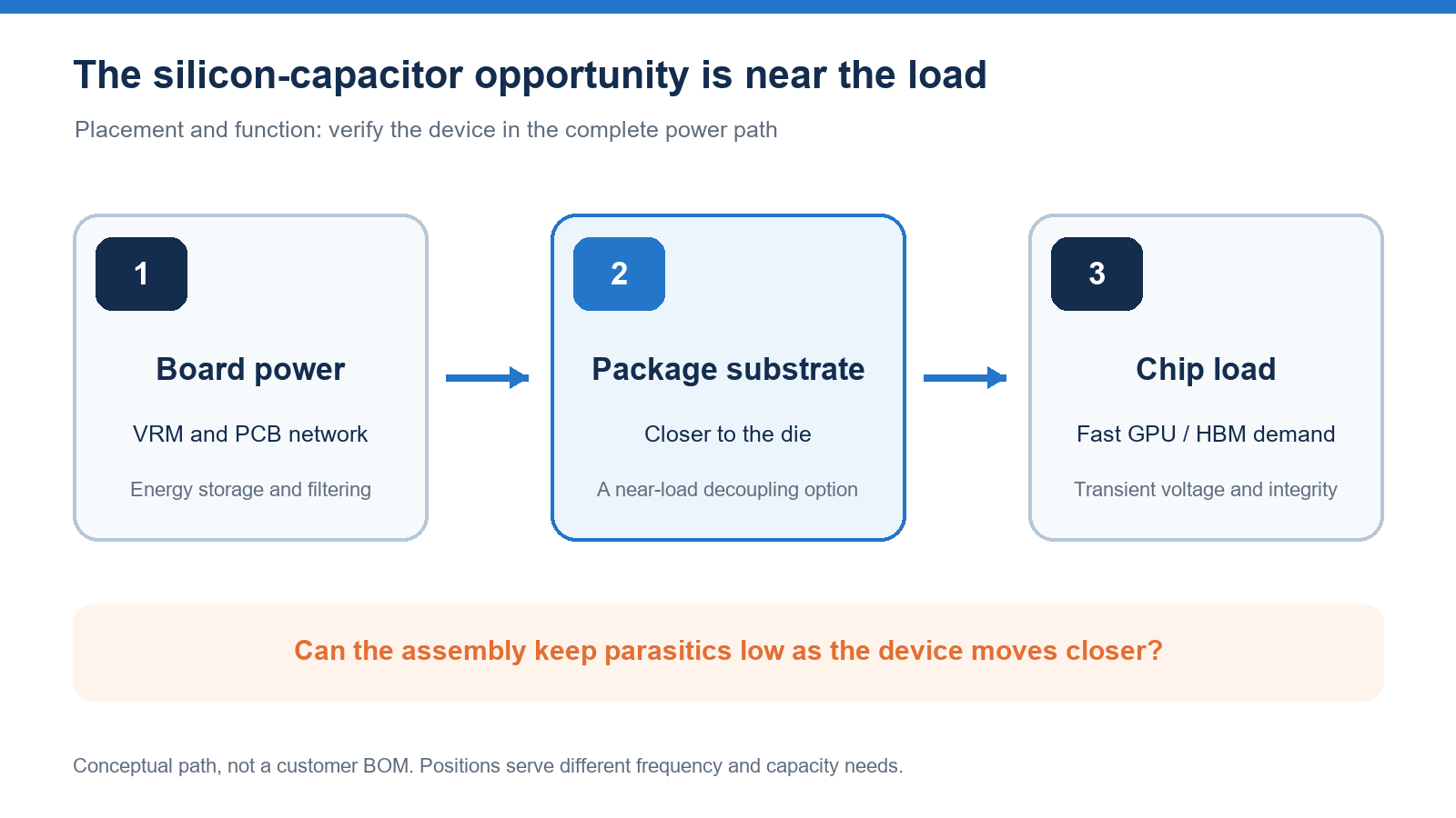
Figure 1. Board, package substrate and chip load are shown as positions in a power path, not as a customer bill of materials. Component requirements differ by position and frequency range.
2. New entrants are starting from different capabilities
Silicon capacitors are established devices. What has become more visible recently is the specificity of the intended application. Launchip's August 2026 announcement describes a 01005-size, 22 nF deep-trench silicon capacitor aimed at 1.6T and 3.2T optical modules. That is a published product and target application; customer qualification and recurring purchases need separate evidence. Samsung's agreement, by contrast, demonstrates a contracted future supply arrangement but does not disclose the customer or part number.
Other companies approach the category from adjacent wafer processes. Etching, deposition, lithography and wafer testing overlap with parts of MEMS and sensor manufacturing. Aosong has announced a wafer-level family including silicon capacitors, chip resistors and chip inductors. Sai Microelectronics lists 3D capacitors among its MEMS manufacturing projects. Such a process base can support development, but it cannot by itself demonstrate a commercial silicon capacitor yield or a stable order book.
The product types also differ. Deep trenches increase effective electrode area. Thin discrete devices can fit height-constrained placements. A silicon interposer containing capacitors becomes part of the package architecture itself. An optical-module maker, a packaging house and a processor designer will therefore qualify different structures against different electrical and assembly conditions.
The move from sample to supply requires control of trench dimensions, sidewall films, leakage, breakdown, wafer-level distribution and batch yield. Once the part is assembled, thinning, bonding or soldering, thermal cycling and failure analysis enter the assessment. A sample can meet a specification while successive production lots still vary too much for a customer to commit to long-term sourcing.
Public information does not yet provide a consistent count of active suppliers, effective capacity or silicon-capacitor revenue across these Chinese projects. Product announcements show where companies are investing; they do not establish a comparable market size.
3. Compare disclosed progress before comparing suppliers
Even apparently similar specifications can be measured at different voltage, temperature, frequency or area definitions. Nominal capacitance is different from effective capacitance in the customer's circuit. The thickness of a discrete part is also different from the height of an assembled interposer. A meaningful comparison starts by identifying the same function and test conditions.
The public record currently supports a more useful comparison of milestones. Samsung has disclosed the value and period of a silicon capacitor agreement, while keeping the counterparty and part number confidential. AP Memory distinguished two S-SiCap routes in its December 2025 announcement: discrete Gen4 devices were in sampling and process validation; its capacitor interposer had completed customer packaging and reliability validation and was entering mass production. Those two statuses should not be merged into one company-wide claim.
Launchip has published a specific size, capacitance and optical-module target. Aosong has announced a device family and process platform. Sai Microelectronics' 2025 annual report states that its 3D capacitor full-process wafer had been developed, had passed customer wafer-level and performance tests, and was undergoing reliability verification. “Achieve mass production” appears as the project's objective, rather than its status at the reporting date. A product release, a passed test, a reliability campaign and a repeat order prove different things.
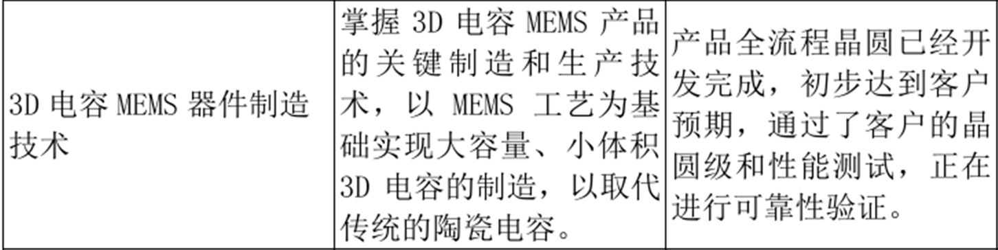
Figure 2. Unaltered excerpt from Sai Microelectronics' 2025 annual report, published in March 2026. The source table is in Chinese; it describes reliability verification as the current stage and mass production as a project goal.
Established suppliers also have experience fitting components into a complete package and power network. Samsung Electro-Mechanics operates across capacitors and package substrates; Murata discusses device behavior alongside power-network design. A customer will ask about placement, interconnects, impedance, temperature and lot variation, not only maximum capacitance density. Chinese suppliers' progress in specific products and tests is visible, but relative performance and market share still require matched tests and comparable sales data.
4. The gates between a sample and a purchase order
Consider a new accelerator package. First the customer measures effective capacitance, ESR, ESL, leakage and voltage withstand at its working voltage, temperature and frequency. Next comes assembly: can the part fit the intended substrate layer or mounting location, and do its thickness, pads and joining method survive the required thermal cycles?
The part must then be assessed with the supply and return paths. A low device ESL can be offset by interconnect inductance. The team measures impedance, voltage droop and ringing under its target transient load and compares the result with the incumbent design. Reliability testing must match the actual size, structure and assembly process.
After a design passes, manufacturing evidence determines the order size. Buyers need distributions within a wafer and across lots, screening rules, yield, capacity, failure analysis, traceability and change control. Those records allow them to estimate the risk of uninterrupted production. Application advice and repeatable batches can matter as much as a strong component curve.
Economics must be assessed at system level too. Wafer processing, test, dicing and packaging make up the device cost, while a substrate or assembly change creates introduction costs for the customer. A higher unit price may be acceptable if nearby decoupling frees space elsewhere or meets a power target that the existing design cannot reach. Public cost and yield data are too limited for a general price ranking; the calculation belongs to each project.
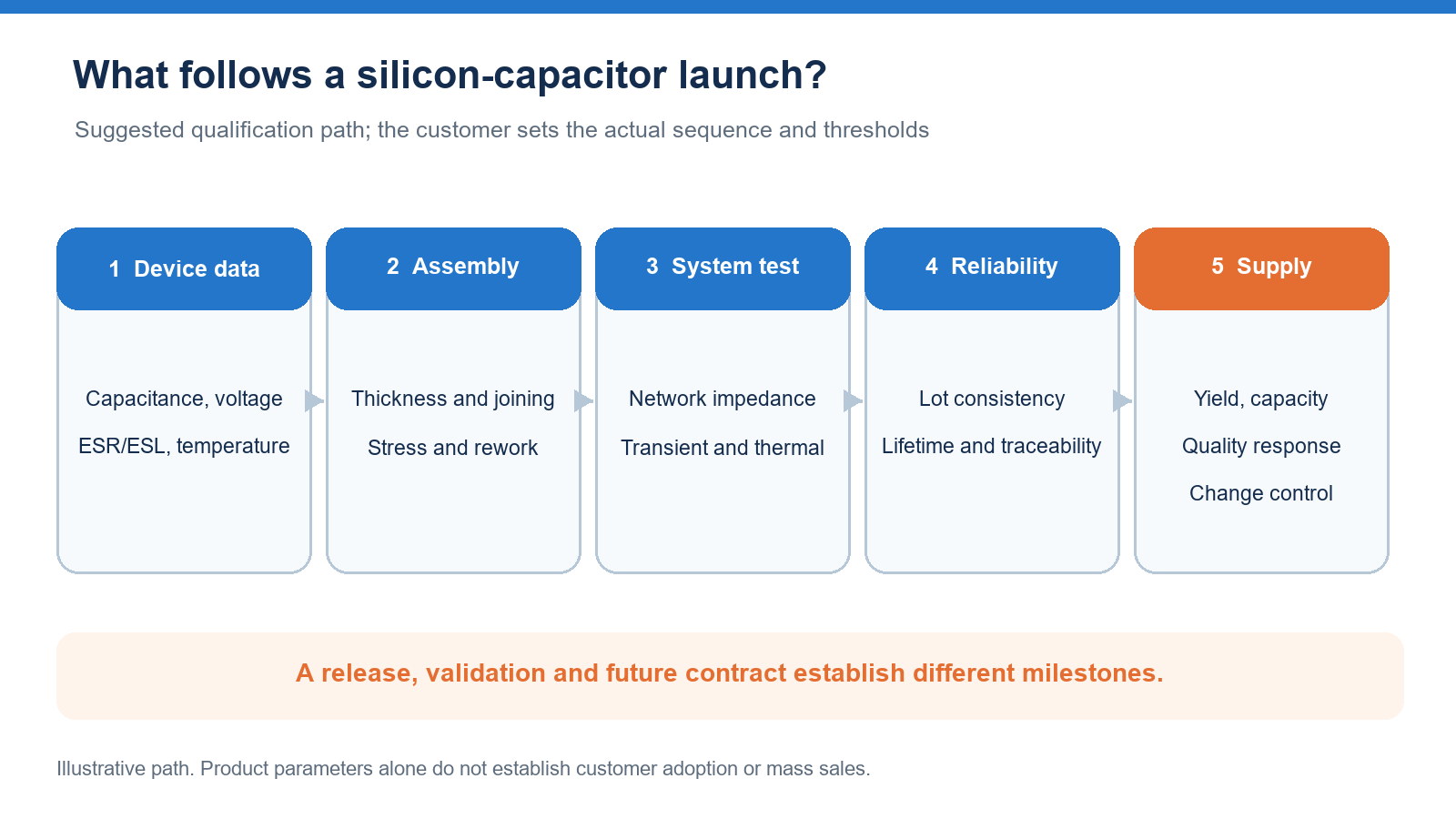
Figure 3. Suggested validation path. The sequence and thresholds depend on the customer's application and packaging design; a release, certification, future contract and shipment are distinct milestones.
5. Where a new supplier can build a record
High-speed optical modules offer one concrete route: develop for a specified size, frequency environment and assembly method, then track qualification through to purchasing. Near-die decoupling in AI processor packages may offer larger opportunities, but it also requires earlier participation in package and power-network design. Other projects with tight thermal, space or assembly limits can begin through joint validation.
The supplier's existing strengths influence its route. A wafer-process company can emphasize customized development and lot consistency. A specialist component designer can concentrate on a few repeatable product families. An established passive-component maker may bring customer access and quality systems, while still needing to extend its service into package-level design. Each route ultimately faces the same test: repeated orders supported by stable quality and delivery.
Useful signals to watch are updated specifications for the same product family, qualification that progresses into actual purchases, and yield and quality records that hold up during expansion. A launch earns a place in technical discussions. Reliable delivery earns a place in the next product cycle.
Source-manuscript claims requiring separate evidence
The Chinese manuscript includes the following additional assertions. This English review retains their existence for cross-language reconciliation but does not treat them as verified findings:
- Silicon-capacitor ESL below 10 pH or as low as 2–3 pH, ordinary MLCC ESL of 100–500 pH, and a two-order-of-magnitude noise-suppression advantage; negligible DC-bias derating, capacitance within ±1% from −55 °C to 175 °C; and thickness below 100 µm as general category-wide characteristics. These need named parts and matched test conditions.
- Samsung's contract as a commitment by an identified AI computing customer; Murata's factory and technology position; and TSMC's silicon-capacitor process integration as described in the Chinese introduction. The cited Samsung disclosure does not name its customer, and the other company-specific statements need current primary-source confirmation.
- A 95% yield for one named domestic firm, an eight-inch pilot line for another, and statements that Chinese suppliers have already entered particular customer supply chains. The named companies and the claimed scope and date are retained in the Chinese source; the available review record does not establish those milestones.
- Approximately US$60 of silicon capacitors per GPU, 30–40 parts per GPU, 20,000–30,000 capacitors per AI-server board, 20–30 or 30–50 silicon capacitors per optical module, and 2026 Chinese incremental-market estimates of RMB 700–900 million and RMB 400–600 million. These numbers need a common bill-of-materials definition, shipment base and calculation. They are not market estimates adopted by this English article.
- Broad forecasts for automotive adoption after 2027–2028 and categorical claims that silicon capacitors always outperform MLCCs in particular environments. Those conclusions require application-specific qualification and market evidence.
This article is for industry discussion. Product status and supply relationships should be checked against the latest manufacturer and customer disclosures before investment, purchasing or part-selection decisions.