
In a traditional wideband radar or communications design, engineers assemble a data relay team on the PCB. The RF front end transmits and receives signals. Separate RF ADCs and RF DACs perform conversion. SerDes inside the converters and FPGA move sampled data over board-level JESD204B/C links. The FPGA handles digital signal processing, while a processor manages control and scheduling. Each chip has a defined role, but as channel count and sample rate rise, clocks, synchronization, and high-speed routing become system bottlenecks.
On June 8, 2026, Altera introduced the Agilex 9 Direct RF-Series SoC FPGA AGRW039, integrating RF data converters, programmable logic, DSP resources, and an Arm processing subsystem in one package. Published specifications list 8 RF-sampling receive ADC channels and 8 RF-sampling transmit DAC channels, each at 10 bits and up to 64 GSPS. Target applications include radar, electronic warfare, high-bandwidth secure communications, and RF instrumentation.
Its impact lies in more than the headline 64 GSPS figure. It attempts to rewrite the wideband RF data path: sampled data that once crossed multiple devices and the PCB begins to remain inside a Direct RF package.
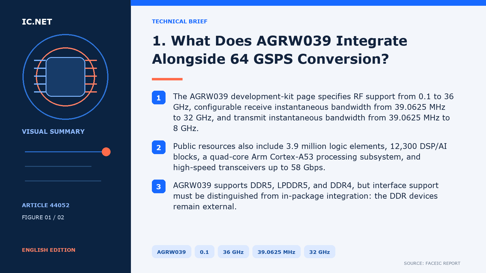
1. What Does AGRW039 Integrate Alongside 64 GSPS Conversion?
The AGRW039 development-kit page specifies RF support from 0.1 to 36 GHz, configurable receive instantaneous bandwidth from 39.0625 MHz to 32 GHz, and transmit instantaneous bandwidth from 39.0625 MHz to 8 GHz. Public resources also include 3.9 million logic elements, 12,300 DSP/AI blocks, a quad-core Arm Cortex-A53 processing subsystem, and high-speed transceivers up to 58 Gbps.
AGRW039 supports DDR5, LPDDR5, and DDR4, but interface support must be distinguished from in-package integration: the DDR devices remain external. Support for DDR5 or LPDDR5 does not mean that either memory is included in the package. Public product information gives package dimensions of 56 mm × 45 mm and says the FPGA portion uses the Intel 7 process. Altera describes the series as a chiplet-based multichip package and specifically references EMIB and AIB. The company attributes low antenna-to-baseband latency to a combination of EMIB/AIB, removal of the added latency from board-level JESD204B/C protocol and transceivers, hardened IP, and the FPGA architecture.
AGRW039 is therefore more accurately described as a single-package, chiplet-based Direct RF SoC FPGA than as a single die performing every function. For the system engineer, the important change is that the RF converter-to-FPGA path no longer depends on a PCB-level JESD204B/C link, not the number of dies inside the package.
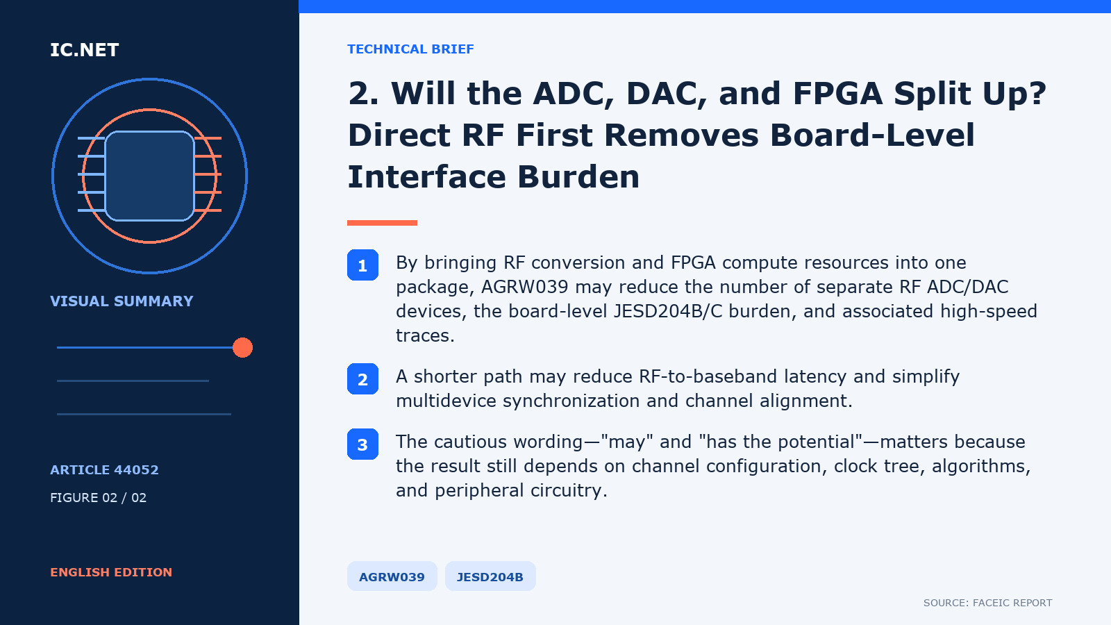
2. Will the ADC, DAC, and FPGA Split Up? Direct RF First Removes Board-Level Interface Burden
In a typical discrete architecture, separate high-speed ADCs, DACs, and FPGAs exchange sampled data over JESD204B/C on the PCB. SerDes is generally integrated in the converter and FPGA rather than existing as a mandatory standalone JESD interface IC. The actual costs are high-speed lanes, reference clocks, SYSREF and synchronization design, multilayer routing, link bring-up, and power.
By bringing RF conversion and FPGA compute resources into one package, AGRW039 may reduce the number of separate RF ADC/DAC devices, the board-level JESD204B/C burden, and associated high-speed traces. A shorter path may reduce RF-to-baseband latency and simplify multidevice synchronization and channel alignment. The cautious wording—"may" and "has the potential"—matters because the result still depends on channel configuration, clock tree, algorithms, and peripheral circuitry.
Direct RF does not erase the RF BOM. LNAs, PAs, filters, switches, limiters, attenuators, and baluns after the antenna remain functions of frequency band, power, noise figure, and linearity. Some applications retain frequency conversion or an IF chain. Clocks, power supplies, configuration storage, external DDR, and cooling also remain.
AGRW039 converges the board-level data path between RF conversion and compute; it does not compress an entire radar into one chip. Device count may fall, while power density, thermal difficulty, and the consequence of a single-point failure become more concentrated.
3. Sixty-Four GSPS Is Not a Universal Answer; 10 Bits Come with Another Test Matrix
Sample rate can create the illusion that the largest number is automatically best. AGRW039's RF ADCs and RF DACs are both 10-bit and operate at up to 64 GSPS. That combination is attractive for radar and spectrum systems prioritizing ultrawide instantaneous bandwidth, frequency agility, channel density, and low latency. It is not sufficient by itself for instruments that prioritize dynamic range, noise floor, spurious performance, and measurement accuracy.
AMD Versal RF Series takes another approach. The VR1602, VR1652, VR1902, and VR1952 integrate 14-bit RF ADCs and RF DACs. Depending on the device, the RF ADC reaches 8 or 32 GSPS, the RF DAC reaches 16 GSPS, and analog input and output frequencies extend to 18 GHz. The devices also integrate programmable logic, AI Engines, and hardened blocks such as FFT/iFFT, channelizers, and LDPC. Altera AGRW039 emphasizes 10-bit, 64 GSPS conversion, RF support to 36 GHz, 32 GHz receive instantaneous bandwidth, and chiplet packaging.
The comparison is not simply 64 versus 32, and AMD's 32 GSPS ADC capability should not be misreported as 32 GSPS for both ADC and DAC. Engineers need ENOB, SFDR, SNR, phase noise, channel isolation, calibration, receive and transmit bandwidth, algorithm mapping, worst-case power, and evidence that the tools and hardened IP reduce development effort. Direct RF competition has moved from an isolated ADC or FPGA metric to a system contest spanning analog performance, compute architecture, packaging, and software.
Discrete architectures will not disappear. They let a customer choose converters, FPGA, and analog front end separately and adjust the BOM for dynamic range, cost, lifecycle, or second-source requirements. A single-package solution provides more integration but less substitution flexibility if one analog parameter or resource mix does not fit.
4. Engineering Samples Exist; a Production BOM Still Has Four Gates
Altera's June 8, 2026 announcement said AGRW039 engineering samples were available and that production devices and development kits were planned for the third quarter of 2026. As of August 13, 2026, the development-kit page marked Offering Status as Production and listed the on-board device order code AGRW039R31F2I2VC. That web status establishes only that the development-kit listing is marked Production; it does not by itself establish broad, stable supply of production AGRW039 devices.
Engineering samples support algorithm porting, RF-chain evaluation, and board prototypes, but they are not equivalent to production release. At least four gates remain. First is analog performance across bands: SNR, SFDR, linearity, channel isolation, and calibration stability. Second is clocking and synchronization: a 64 GSPS path is highly sensitive to sampling-clock jitter and multichannel phase consistency. Third is power and cooling: fewer devices do not remove power, but concentrate heat in and around a dense package. Fourth is software and IP: whether DDC, DUC, FFT, beamforming, and data movement converge on timing, resources, and power in the Quartus toolchain determines whether data-sheet capability becomes a deliverable system.
Procurement also cannot compare AGRW039 price with a simple sum of ADC + DAC + FPGA. The system model must include clocking, power, PCB layers, cooling, tools, IP licenses, algorithm migration, qualification time, board-spin risk, and lifecycle supply. Higher integration can raise the unit price while lowering system cost; fewer chips do not guarantee a lower total project cost.
Conclusion: Direct RF Moves the Board-Level Data Wall into the Package
AGRW039 sends a clear industry signal. Wideband radar, electronic-warfare, and advanced-communications systems are moving from separately selecting an RF ADC, RF DAC, and FPGA toward selecting a programmable compute platform with RF data conversion at its input.
Discrete converters and conventional FPGAs will retain important markets in precision instruments, unusual frequency bands, cost-sensitive equipment, and programs that prioritize multisourcing or modular upgrades. In systems that emphasize instantaneous bandwidth, real-time processing, channel density, and SWaP, however, the architectural appeal of a Direct RF SoC FPGA is increasing.
AGRW039 is not primarily competing for one ADC socket. It is competing for the resource-intensive, difficult-to-tune JESD204B/C board link that crosses the PCB in a conventional RF data chain. Only after production devices, analog performance, thermal design, tools, and lifecycle supply pass project validation will the architectural advantage enter a production BOM.
Disclaimer: This article is for industry discussion only and does not constitute investment, procurement, or part recommendations. Product parameters, supply status, and project suitability are subject to the latest manufacturer information and actual validation results.